| No | Task | Example | Capa | Solution | Method |
|---|---|---|---|---|---|
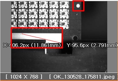
| 1 | Gold bump size (CD) X, Y 2D dimension | 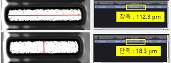 |
100% | 2D Camera algorism program development | 2D Camera Inspection |
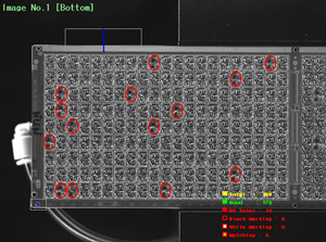
| 2 | Back Side Marking | 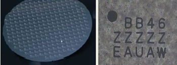 |
100% | 2D Camera algorism program development | 2D Camera Inspection |
| 3 | Solder bump Pattern/Ball Inspection | 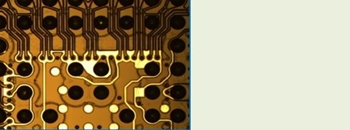 |
100% | 2D Camera algorism program development | 2D Camera Inspection |
| 4 | Sensor Chip Both Sides Inspection | 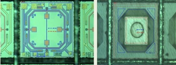 |
100% | 2D Camera algorism program development(both sides) | 2D Camera Inspection |
| 5 | EBR | 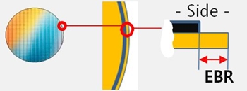 |
100% | 2D, CCD of alignment camera | 2D Camera Inspection |
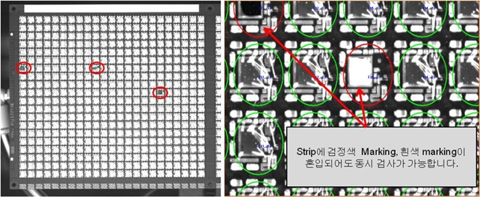
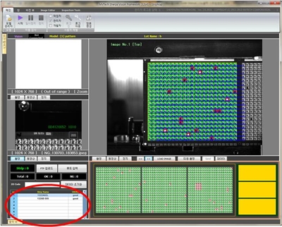
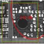
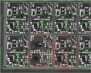
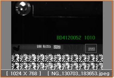
Score 관리를 통한 Chip의 이상 유무를 확인할 수 있습니다.
등록한 Pattern
[ score = 100 ]
Chip이 없을 경우
[ score = 20 ]
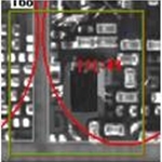
Wire 불량
[ score = 49 ]
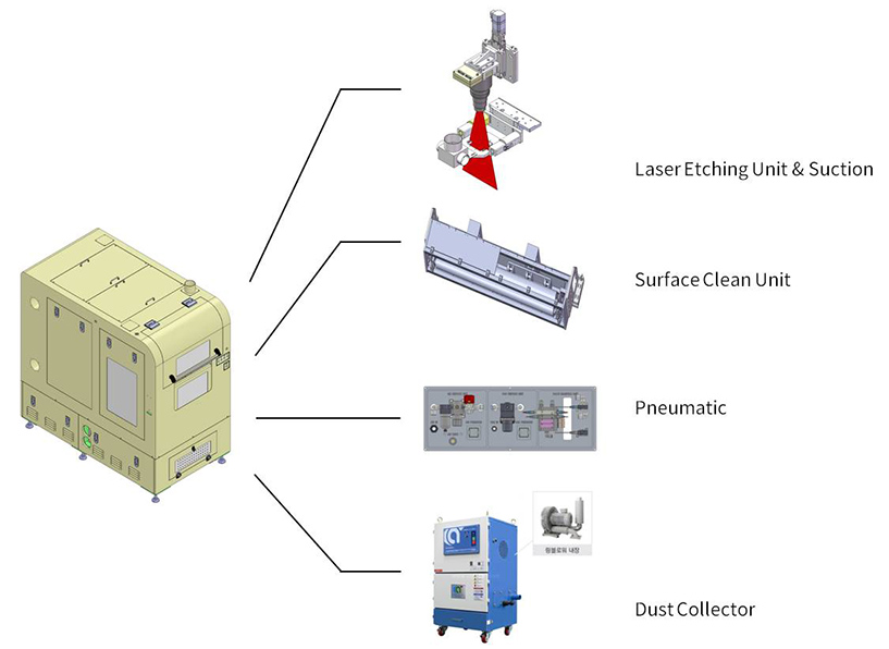
| No | Process | Function |
|---|---|---|
| 1 | Loading | Manual |
| Index Robot | ||
| 2 | Align | Optional |
| 3 | Laser Process Unit | Laser Etching (Green or IR Laser) |
| Dust Suction (Blower) | ||
| 4 | Clen Process | Sticky Roller |
| Blower and Suction | ||
| Brush | ||
| 5 | Unloading | Manual |
| Index Robot |
| Application | Surface Etching |
|---|---|
| Substrate input sheet size | 80mm x 80mm |
| Thickness | 5 ~ 10mm |
| Cell size | 25mm x 25mm ~ 300mm x 300mm |
| Clean class |
Idle : Class 1000 Run:Class 10000 |
| Laser | Green Laser or IR Laser |
| Etching accuracy | Accuracy of Green Laser: ≤±100µm |
| Etching speed | Green laser Etching : Max 500mm/s |
| LASER & OPTICS UNIT |
|
|---|---|
| MECHANICAL UNIT |
|
| PERIPHERAL EQUIQMENT |
|
| OPTIONAL |
|
Wafer ID Marking M/C는 Wafer의 Top side에 wafer ID를 Marking하는 System 장비 입니다.
고속 가공이 가능하며, 사용자의 편의에 따른 프로그램 변경이 용이한 Wafer ID Marking 솔루션을 제공합니다.
Wafer scanning (mapping) 🠖 Wafer loading 🠖 D cut aligning 🠖 Laser marking 🠖 OCR & 2D barcode scanning 🠖 Wafer unloading
| Item | Specification | |
|---|---|---|
| Wafer Size | Min 6” – Max 8” | |
| M/C Size | 1800 * 1200 * 2000(H) (mm) | |
| Cassette Path line | 900 (SEMI Standard) | |
| Number of port | 2 Port | |
| Accuracy | ±0.1mm | |
| Tact time | < 30s | |
| Utility | Power | AC220V, 단상 50/60Hz, 25A |
| Vacuum | -400mmHg 이상 | |
| CDA | 5kgf/cm^2, 45l/min | |
| Option | Carrier ID Reader(RFID) | |
| Wafer mapping unit | ||
| FFU(ULPA Filter) | ||
| Ionizer장착 (SEMI Standard) | ||
| CIM | ||
| Technical Specification | |
|---|---|
| Laser Type | Green Laser (IR Laser optional) |
| Wavelength | 532nm |
| Min Beam Diameter | < 10um |
| Beam Quality M2 | < 1.2 |
| Pulse Frequency | 10-200 kHz |
| Output Power | 10 Watts |
| Repetition Accuracy | 2um |
| Cooling System | Water-cooled |
| Fθ Marking Field Size | 50mm x 50mm |
| Laser Safety Level | Class 1 |
| Electrical Connection | 220V (±10%), 50/60Hz, 20A |
| Power Consumed | 5Kw |
| Warranty Coverage (Parts & Labor) | 1-year |
| Laser Safety Compliance | FDA(CDRH) |
| Running Temperature | 15-35℃ |
| Marking Letter | 7-10 Text |
| Warranty | 1year & 20,000h |